Production line introduction
- Current position >>
- Production line introduction >>
- Production process flow
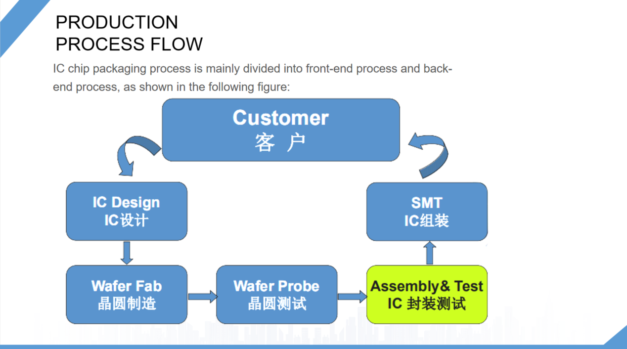
IC chip packaging technology
The IC chip packaging process is mainly divided into the front process and the back process, as shown in the following figure:
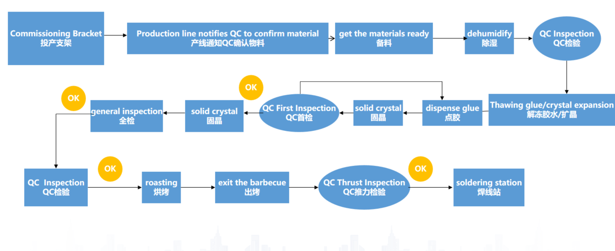
Solid crystal production process
Solid crystal process process, detailed as shown in the following figure:
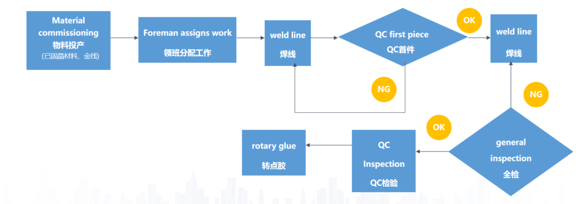
Welding process flow
Welding process description
The welding process of SMD is to burn a ball first, and then press the first point on the wafer electrode, and then pull the gold wire to the corresponding secondary solder joint support, press the second point and burn the gold wire. (Note: The welding wire is the key link in SMD packaging technology, and the process needs to pay attention to monitoring the shape of the welding wire arc, the shape of the solder joint and the gold wire tension and the gold ball thrust).
Welding parameters: According to different products and different machines and equipment, respectively debug welding power, welding pressure and welding time.
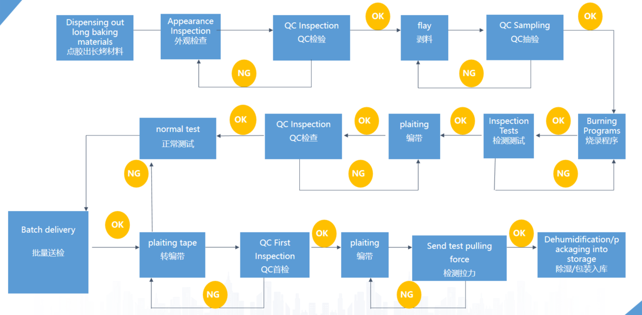
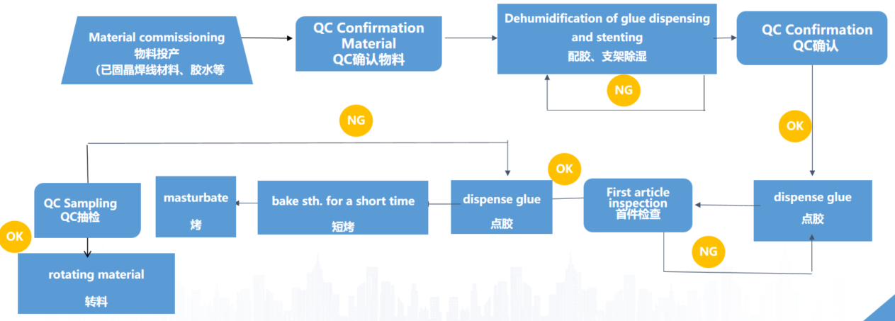
Dispensing process flow
Dispensing package instructions:
The package of the patch adopts the form of dispensing. The dispensing process is to inject liquid silica gel into the bracket bowl, and then bake the silica gel to cure and form.
Hot glue baking condition: 135℃/2H
Note: The product with good glue will be baked within 30min.
Control IC product specifications
Appearance inspection: Pick out the defective products and appearance defective products at the front station (such as more glue, less glue, leakage point, overflow P/N foot glue, etc.)
Stripping: The bracket is a PCB board, and the stripping machine is required to complete the separation into a single product.
Testing: testing functional parameters, and sorting products according to customer requirements.
Tape braiding: counting the finished product for use by the customer.
Note: For each volume of 4K, all tape materials should be attached with beautiful paper and indicate the quantity, product model, tracking number, BIN number and job number code)
Packaging: After material dehumidification is complete, according to the requirements of the dispatch order and customer requirements, print labels according to the correct label printing method.
